
TSMC N2 and CoWoS: 70% Yields and 1.0M Wafer Demand Shape the Global AI Supply Line
On July 16, 2026, Taiwan Semiconductor Manufacturing Company reported a record second-quarter revenue of NT1.27 trillion, or approximately 39.62 billion, representing a 36% year-over-year increase that exceeded its own upper-bound guidance of $40.2 billion. This financial surge proves that global demand for advanced TSMC AI chips remains entirely unsated by existing silicon capacity. The market is now looking beyond the top-line numbers to parse the exact manufacturing yield rates, advanced packaging limits, and capital expenditures that govern the physical deployment of machine learning clusters.
Key Takeaways
- Second-quarter revenue of NT$1.27 trillion establishes a historic high-water mark for semiconductor demand, driven by unrelenting hyperscaler procurement.
- CoWoS packaging capacity remains the primary hardware throttle, with total 2026 demand approaching 1.0 million wafers against a capped supply.
- Trial production of the 2nm N2 node has surpassed a 70% yield rate, cementing TSMC’s manufacturing advantage over competitors.
- Capital expenditure guidance tracking at the high end of 52 billion to 56 billion signals aggressive global cleanroom expansion through late 2026.
Architecture & Packaging
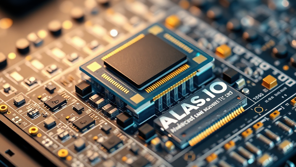
Advanced packaging dictates the maximum performance of modern TSMC AI chips. Multi-die processors cannot rely on traditional printed circuit boards because interconnect density is too low. Instead, system architects utilize Chip-on-Wafer-on-Substrate (CoWoS) technology to bond logic dies and high-bandwidth memory (HBM) stacks. This integration relies on a sub-micron silicon interposer. The interposer contains ultra-fine copper wires that allow terabytes-per-second communication speeds.
Currently, TSMC supports two distinct advanced packaging variations. First is CoWoS-S, which uses a solid silicon interposer. It provides maximum routing density but suffers from reticle limits. The second is CoWoS-L, which utilizes localized silicon bridges embedded within an organic substrate. This hybrid approach allows designers to stitch together multiple logic dies that exceed standard lithography reticle limits to produce complex TSMC AI chips. It is the foundation for Blackwell accelerators.
Silicon real estate is tightly packed. A standard Blackwell dual-die package spans over 1,600 square millimeters of silicon, pushing the limits of physical assembly. Managing such vast areas introduces mechanical strain during thermal cycling. Substrates can warp. Micro-bumps can crack. To mitigate this risk, TSMC uses specialized underfill materials to stabilize the package. These materials must absorb stress without expanding.
Memory integration adds further physical complexity. High-bandwidth memory stacks sit millimetric distances from the main logic processor. This proximity is necessary for high signal integrity. However, it concentrates heat. If a memory stack overheats, the system throttles performance. Current designs integrate eight to twelve HBM3e stacks around the logic cores of advanced TSMC AI chips. This layout demands precise placement.
The physical dimensions of these TSMC AI chips present a major yield challenge. Large dies are statistically more likely to contain defects. By splitting a massive processor into smaller chiplets, manufacturers can improve raw silicon yield. However, the cost of packaging these chiplets together on an interposer remains incredibly high. Silicon bridge alignment requires sub-micron precision. One misaligned micro-bump ruins the entire assembly.
In my view, relying on localized silicon bridges remains a high-stakes compromise that complicates signal integrity in favor of physical scaling.
Alternative structures are emerging. System designers are looking at alternative packaging technologies to avoid long queues at TSMC. Some smaller designers have successfully modified their physical layouts to use Intel’s EMIB technology as a backup. This shift alters the unit cost structure of custom ASICs. For a deeper look at how alternative packaging strategies change the financial equation for hardware developers, analyze the Best AI Chip Stocks: 3 Secret Winners of CoWoS Delay.
Ultimately, physical integration limits determine compute density. Standard logic shrinks no longer provide the necessary performance boosts. This reality elevates the importance of 2.5D and 3D silicon stacking. If TSMC cannot scale its packaging lines, the deployment of next-generation TSMC AI chips will slow down regardless of wafer fab capacity. Hardware limits are absolute.
Perf/W & Benchmarks
A 15% density gain over the N3E node defines the physical structure of TSMC’s 2nm N2 process. In workload-specific benchmarks, this structural shift translates directly into major performance-per-watt (perf/W) improvements. Standard silicon designs running on the first-generation GAA nanosheet architecture show a 10% to 15% performance increase at identical power levels, elevating the benchmarks for TSMC AI chips. Alternatively, they can deliver a 25% to 30% reduction in power consumption while maintaining the same operational frequency. These metrics are vital for operators of hyperscale data centers.
For high-performance computing, the efficiency gains of these TSMC AI chips reshape the operating economics of large cluster installations. Power delivery networks are highly optimized on N2. By implementing super-high-performance metal-insulator-metal (MiM) capacitors, TSMC has reduced voltage drop during sudden compute spikes. This stability allows the processor to run closer to its voltage ceiling without crashing. It prevents computational dropouts during heavy training runs.
Let us compare the raw processing power of N2 and N3E silicon directly. A wafer containing N2 TSMC AI chips displays a mixed transistor density exceeding 300 million transistors per square millimeter. This dense packing allows developers to fit larger SRAM caches directly onto the logic die. In cache-heavy workloads, such as large language model inference, on-chip memory density is paramount. Accessing data from off-chip memory consumes up to one hundred times more energy than reading from local SRAM.
This architectural shift is visible in recent hardware benchmarks. High-performance accelerators fabricated on the N2 node process up to 35% more tokens per second per watt compared to older 4nm systems on transformer-based workloads. These results are achieved through the Nanoflex design feature. Nanoflex allows hardware architects to mix high-performance logic cells with ultra-low-power cells in the same physical layout. It optimizes the power footprint of non-critical scheduling blocks.
Is this performance scaling sufficient to justify the massive capital outlay required for 2nm design cycles? In my view, the thermal and power savings of the N2 node represent the only viable path forward for hyperscalers facing strict regional grid constraints. Without these efficiency gains, building out million-GPU clusters would require dedicated gigawatt-scale power substations.
The efficiency of these TSMC AI chips also impacts edge applications. Lower switching power extends battery life in client devices. It also reduces thermal output in tight physical enclosures. System developers can design passively cooled enclosures for inference hardware. This flexibility is essential for deploying TSMC AI chips in industrial robotics and automotive control units.
Yield, Cost, and Capacity

Yields and Premium Pricing for TSMC AI chips
A 70% yield rate in trial production of the N2 node represents an unexpected manufacturing milestone for TSMC. This percentage exceeds initial street expectations for a gate-all-around architecture. Yields are high. High initial yields allow the foundry to maintain strong pricing power. Consequently, TSMC has set the price of a single 2nm wafer at approximately 30,000. This price represents a 50% premium over the 20,000 cost of a 3nm wafer.
These financial parameters demonstrate that the cost of fabricating TSMC AI chips is rising alongside density. This pricing strategy directly impacts the unit economics of TSMC AI chips. System developers must absorb these silicon costs or pass them to enterprise buyers. For advanced custom silicon, the high wafer cost can be prohibitive. However, some design modifications can radically lower these expenses. Developers can review how Global Workspace Theory AI Slashes 2nm ASIC Costs by 90% to understand the structural changes enabling cheaper custom processors.
The current financial metrics for TSMC’s leading-edge manufacturing illustrate this dynamic clearly:
| Process Node | Wafer Price (USD) | Est. Target Yield (July 2026) | Primary Customers | Nanosheet Adoption |
|---|---|---|---|---|
| N3E (3nm) | $20,000 | ~80-85% | Apple, Nvidia, AMD | No (FinFET) |
| N2 (2nm) | $30,000 | >70% | Apple, Qualcomm, MediaTek | Yes (GAA) |
| N2P (2nm+) | ~$33,000 (est.) | Trial Phase | Next-Gen Hyperscalers | Yes (Backside Power) |
Wafer capacity is expanding rapidly in Taiwan to accommodate these designs. In Hsinchu’s Baoshan district, Fab 20 has transitioned its P1 line into full volume production, while the P2 line has completed tooling. Simultaneously, Fab 22 in Kaohsiung is installing next-generation lithography scanners. Together, these four sites are projected to produce 60,000 wafers per month by late 2026. This massive volume is essential to satisfy the order books of major TSMC AI chips consumers.
However, packaging capacity remains a bottleneck. While silicon wafer fabrication is highly optimized, advanced packaging lines are oversubscribed. Lead times for CoWoS-L packaging range between 52 and 78 weeks. TSMC is aggressively addressing this issue. The company is scaling its advanced packaging output from 35,000 wafers per month in late 2024 to a projected 130,000 wafers per month by the end of 2026. Despite this 4x expansion, the capacity is already fully booked.
This supply deficit creates high-stakes allocation battles for TSMC AI chips. Nvidia has secured approximately 60% of total CoWoS output for 2026, equivalent to 800,000 to 850,000 wafers. This massive allocation locks up capacity for both Blackwell Ultra and next-generation Rubin architectures. Competitors are left fighting over the remaining 40% of the supply. AMD holds just 11% of the allocation, which limits its ability to scale its MI350 accelerators.
My analysis indicates that TSMC’s premium pricing on the N2 node is a calculated strategy to offset the immense capital depreciation of its overseas fabs. The company’s massive 52 billion to 56 billion capital expenditure budget for 2026 requires elevated gross margins to maintain historical profitability. By charging $30,000 per wafer, the foundry can ensure its domestic lines remain highly profitable even as overseas projects dilute margins.
For enterprise buyers, the yield curves are the most critical metric. High yields on the N2 node mean fewer defective dies per wafer, lowering the real cost per functional chip. If TSMC can push N2 yields past 80% by early next year, it will solidify its lead over Intel’s 18A process, which currently reports an 85% yield but lacks comparable high-volume production experience. The race to deliver affordable TSMC AI chips hinges on this specific operational metric.
Supply Chain Dynamics

Geopolitics and logistics dictate the global distribution of advanced silicon. On July 2, 2026, Taiwan’s Ministry of Economic Affairs approved a massive $20 billion capital injection into TSMC’s Arizona subsidiary. This approval is the sixth. It brings the total cleared US funding to $44 billion. The capital will construct a second 12-inch wafer fab and an advanced packaging plant. Taiwan remains the hub. Despite this expansion, the geographic concentration of TSMC AI chips remains heavily skewed toward East Asia.
The Taiwanese government has been open about this structural imbalance. Minister of Economic Affairs Kung Ming-hsin stated that the United States is highly unlikely to match Taiwan’s domestic production capacity. To support his point, Kung highlighted a stark number. TSMC has planned or built 16 separate fabrication and packaging facilities within Taiwan. This local ecosystem cannot be easily duplicated abroad. The highly specialized labor, materials suppliers, and cleanroom engineering firms reside in a tightly integrated physical cluster.
This geographical concentration creates operational risks for buyers of TSMC AI chips. In response, customers are actively exploring backup packaging options. Because CoWoS capacity remains oversubscribed, orders are spilling over to alternative packaging providers. Companies are qualifying Intel’s EMIB packaging as a secondary source. Additionally, Taiwanese outsourced semiconductor assembly and test (OSAT) firms are seeing historic demand. Analysts expect ASE advanced packaging sales to double by the end of 2026.
This distribution of packaging orders helps mitigate supply chain bottlenecks. However, transferring a design from CoWoS to a competitor’s process is not simple. It requires extensive engineering redesigns and rigorous physical validation. If a designer must pivot quickly due to a supply shock, they face significant time-to-market delays. System architects designing TSMC AI chips must weigh this packaging flexibility against raw performance.
The supply chain for advanced packaging also involves specialized materials. High-bandwidth memory chips are a key component. Currently, SK Hynix maintains a close relationship with TSMC, utilizing its CoWoS platform to secure market dominance over Samsung in the AI memory space. This partnership ensures that SK Hynix memory is tightly integrated into the biggest TSMC AI chips. Any disruption in this specific memory supply line would instantly halt the delivery of high-end accelerators.
From my perspective, the rising cost of overseas manufacturing will inevitably force TSMC to implement localized pricing structures. Buyers wanting chips fabricated entirely within the United States will pay a premium to cover the higher operational costs of the Phoenix fabs. This premium will split the market for TSMC AI chips into distinct regional pricing tiers.
Forward Vector
Monitoring the progress of the N2P node ramp during this half of 2026 constitutes the primary checkpoint for hardware analysts. This node introduces backside power delivery, a technology that separates power routing from signal routing to improve efficiency. If TSMC executes this transition smoothly, system designers will secure an immediate 10% efficiency gain without changing their logic architectures. However, any manufacturing delay at Fab 20 will trigger downstream product delays across the entire tech sector.
Execution risks are highly concentrated around advanced packaging lines. While wafer starts are plentiful, the lack of sufficient CoWoS capacity remains an active bottleneck for TSMC AI chips. If the Chiayi AP7 packaging plant suffers construction delays, hyperscalers will see their accelerator allocations cut. Investors must monitor quarterly capital expenditure updates to see if TSMC raises its 2026 budget past the current $56 billion ceiling. A capex increase would signal higher commitment to packaging expansion.
Geopolitics present the second major checkpoint. The implementation of phase-two tariffs or stricter export controls on TSMC AI chips could disrupt supply networks. If regulatory bodies restrict advanced packaging services on Taiwanese soil, hyperscalers will face a severe supply crunch. The industry’s reliance on a single island for advanced assembly creates a fragile foundation. This geographic risk is prompting major chip designers to diversify their physical supply chains.
This diversification effort is already underway. Major designers are qualifying alternative packaging sources to protect their product roadmaps. Defect mitigation is critical. If these alternative packaging avenues fail, developers face severe deployment delays. In extreme cases, design errors can delay chips for years. For instance, the Nvidia AI chip delay: Critical failure pushes Kyber to 2028 demonstrates the high cost of packaging and architectural missteps under tight development cycles.
Hyperscalers are also developing custom ASICs to bypass third-party bottlenecks. Meta is preparing to launch its custom Iris chip, while Alphabet is actively commercializing its TPU capacity through neocloud providers. These proprietary designs are optimized for specific internal workloads. They allow software firms to reduce their dependence on standard commercial GPUs. If these custom chips succeed, the market share of general-purpose TSMC AI chips may shift toward specialized internal processors.
In my view, the success of the AI infrastructure cycle over the next 18 months depends entirely on advanced packaging yields rather than raw transistor scaling. If packaging throughput fails to keep pace with demand, the massive capital investments of hyperscalers will fail to generate expected returns, triggering a valuation correction across the technology sector. The physical limits of silicon assembly are now the ultimate arbiters of software progress.
Frequently Asked Questions
Why is CoWoS packaging a bottleneck for TSMC AI chips?
CoWoS advanced packaging is a bottleneck because it requires a highly complex multi-die integration process that cannot keep pace with the massive tripling of global hardware demand. To resolve this, TSMC is aggressively scaling production to reach 130,000 wafers per month by the end of 2026, yet the capacity remains oversubscribed by major players. As a result, developers are experiencing lengthy lead times of up to 78 weeks for these critical TSMC AI chips.
How much does a 2nm wafer cost compared to a 3nm wafer?
A single 300mm wafer fabricated on TSMC’s 2nm N2 process node costs approximately 30,000, which represents a 50% pricing premium over the 20,000 cost of a 3nm wafer. This steep pricing increase reflects the manufacturing complexity of transitioning from traditional FinFET transistors to next-generation gate-all-around nanosheet architectures. These elevated manufacturing costs directly influence the overall system economics of advanced enterprise AI hardware.
What is TSMC’s total capital investment in its Arizona fabs?
Following a massive $20 billion capital injection approved in July 2026, TSMC’s total authorized investment for its Phoenix, Arizona campus has reached $44 billion. This capital is allocated to build out a second 12-inch wafer fabrication plant and an advanced packaging facility on the site. However, Taiwan will maintain the vast majority of advanced production capacity, as the company operates 16 fabrication and packaging plants domestically.