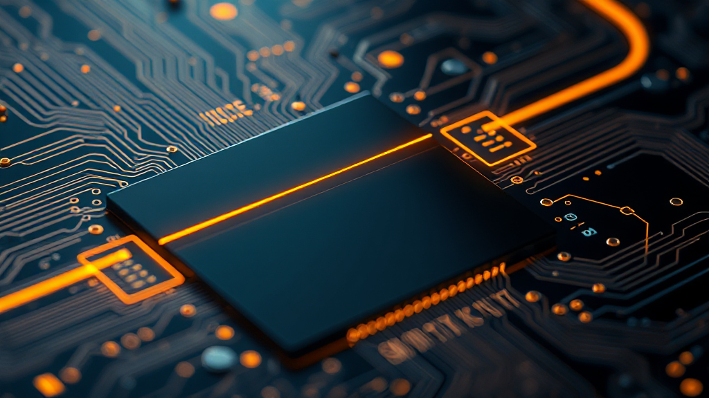
Samsung 2nm: Anthropic Custom Chip Talks Reshape Advanced Packaging Economics
On July 2, 2026, reports emerged that Anthropic had initiated early-stage discussions with Samsung Electronics to manufacture its first proprietary silicon[1][2]. The global land grab for custom AI chips has officially extended to the Claude creator, highlighting how frontier AI laboratories are shifting their attention from software optimizations to direct silicon control[3][4]. By evaluating Samsung’s next-generation 2-nanometer (SF2) gate-all-around (GAA) process node[2][5], Anthropic hopes to construct a dedicated accelerator stack that diminishes its complete financial dependency on Nvidia’s dominant pricing[4][5]. This strategic transition aims to structurally alter the unit economics of hosting frontier models[4].
Key Takeaways
- Anthropic is evaluating Samsung’s 2-nanometer (SF2) gate-all-around foundry process to build its first custom AI chips.
- The hire of OpenAI chip veteran Clive Chan signals that Anthropic is actively assembling a team dedicated to custom AI chips development.
- Samsung’s vertically integrated “one-stop” model offers a unified pipeline for logic fabrication, advanced HBM, and 2.5D packaging.
- This hardware initiative directly mirrors OpenAI’s recent release of its Broadcom-designed “Jalapeño” inference processor.
Architecture and Advanced Packaging for custom AI chips
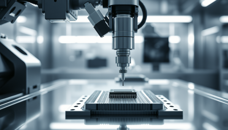
Developing custom AI chips requires a complete rethink of physical transistor geometries. Samsung relies on its proprietary Multi-Bridge Channel FET (MBCFET) gate-all-around (GAA) architecture to drive its 2nm SF2 and SF2P foundry offerings[2][4]. Traditional FinFET layouts restrict current control to three sides of the channel. In contrast, GAA nanosheets wrap the gate electrode completely around the conducting channel[6]. This structural improvement minimizes sub-threshold leakage currents. It also optimizes voltage scaling down to sub-0.7V ranges, which is essential for high-performance computing cards. For custom AI chips running massive transformer architectures, this physical level of control translates directly to higher active operating frequencies within a given thermal envelope.
The transition to GAA at the 2nm node is not merely a marketing exercise. As standard cell heights shrink, conventional FinFETs fail to deliver the necessary drive current without expanding the physical footprint of the cell. Samsung’s SF2 process delivers a reported 12% performance increase and a 25% power reduction compared to its 3nm GAA predecessor[7]. For engineers designing custom AI chips, these physical parameters allow for the integration of larger execution pipelines. They can fit more matrix multiplication engines into the same silicon footprint. Physical layout designers can dynamically alter the width of the nanosheets within a single design block. This capability allows them to trade off leakage for switching speed where it matters most, such as in high-activity arithmetic logic units (ALUs).
In a GAA transistor, the vertical stacking of nanosheets determines the effective width of the channel. A wider nanosheet provides more drive current, enabling faster switching speeds but increasing dynamic power consumption. Conversely, narrower sheets minimize static power. In standard cell designs at the 2nm node, this optimization is handled at the layout level, allowing Anthropic’s team to balance the power-performance trade-offs of key logic blocks. This level of granular tuning is impossible when deploying standard workloads on general-purpose hardware. By controlling the physical nanosheet layers, engineers can construct custom AI chips with execution blocks optimized for low-precision INT8 or FP8 matrix operations.
Silicon scaling faces a hard wall at the physical reticle limit, which hovers around 858 square millimeters. To bypass this barrier, custom AI chips must rely on advanced heterogeneous packaging. Samsung addresses this through its “Cube” advanced packaging portfolio[8][9]. The I-CubeS platform uses a high-density silicon interposer to link the central logic die with multiple High Bandwidth Memory (HBM) stacks[10][11]. This setup provides the immense memory bandwidth required for rapid model parameter retrieval. Alternatively, Samsung’s I-CubeE uses localized silicon bridges embedded within an organic substrate[10][11]. This method lowers fabrication costs while preserving critical high-speed interconnect routing. For ultra-dense configurations, the X-Cube platform uses 3D vertical stacking via through-silicon vias (TSVs) to place logic directly over SRAM caches[12][10].
For custom AI chips, integrating high-density logic with HBM represents the primary technical challenge. Memory access bottlenecks frequently stall high-performance processors during large model inference operations. To prevent this, the die-to-die (D2D) interface must maintain extreme routing density with minimal parasitics. Samsung’s advanced packaging utilizes micro-bumps at tight pitches to bridge the physical gap between the logic die and the memory stacks[11]. This physical proximity ensures that data can move across the interposer at multi-terabyte-per-second speeds. For Anthropic’s future designs, leveraging this integrated interposer structure is the only way to meet the latency demands of real-time conversational agents.
Anthropic’s architectural ambitions are supported by strategic engineering acquisitions. In June 2026, the company recruited Clive Chan, widely recognized as the second hardware engineer hired into OpenAI’s in-house silicon division[13][14]. Chan brings direct expertise in managing complex co-design projects, having previously worked on Tesla’s Autopilot ASIC and OpenAI’s Broadcom-partnered chip program[15][14]. His team must define the internal bus architectures and memory controller interfaces for these custom AI chips. A central design challenge involves optimizing the die-to-die interconnect. The design must handle the vast aggregate bandwidth required to pool multiple accelerators within a server rack without introducing destructive latency penalties.
Performance-per-Watt and Workload-Specific Benchmarks
General-purpose graphics processing units carry immense overhead. When executing deep learning workloads, these processors utilize substantial silicon area for graphics pipelines and double-precision float calculations that transformer models do not require. By focusing on custom AI chips, Anthropic can strip away non-essential execution blocks. The resulting silicon can be dedicated entirely to low-precision matrix multiplication and high-speed memory fetching. Autoregressive inference represents a memory-bandwidth-bound task. The processor must stream billions of weights from off-chip memory into the local execution registers to generate each individual token. Under these workloads, peak compute capability is often less important than the local memory-to-logic execution path.
This performance-per-watt gap is the primary reason why leading AI labs are pursuing custom AI chips. On June 24, 2026, OpenAI and Broadcom announced “Jalapeño,” a custom inference ASIC optimized specifically for large language model inference[16][17]. Early testing shows that Jalapeño delivers performance-per-watt that exceeds standard accelerators[18]. By narrowing the hardware focus to autoregressive transformers, OpenAI expects to slash operational costs significantly[17]. A detailed analysis of OpenAI’s strategy shows that this custom chip slashes LLM deployment costs by 50% [OpenAI Custom Chip Slashes LLM Costs by 50%]. Anthropic faces identical economic realities. Its Claude 3.5 Sonnet model runs on a complex combination of Nvidia GPUs, Google TPUs, and AWS Trainium[1][19].
Inference chips require lower power envelopes than training chips. While a training accelerator like Nvidia’s Blackwell requires upwards of 1,200 watts per socket and relies on liquid cooling, an inference-focused ASIC can operate comfortably within a 250-to-400-watt envelope under passive or standard air cooling. OpenAI’s Jalapeño highlights this divergence[18][17]. Designed specifically for LLM inference, it cuts out the high-speed NVLink interconnects and general-purpose cache hierarchies required for distributed training. For Anthropic, designing an inference-first custom chip would directly address the scaling costs of high-volume API requests, which represent the bulk of their recurring operational expenses.
Designing custom AI chips allows Anthropic to construct specialized matrix-multiplication kernels that directly match the dimension shapes of its internal model architectures. If Claude utilizes specific Mixture of Experts (MoE) routing protocols, the hardware can allocate dedicated routing logic on-chip. This design choice bypasses the standard software compilation overhead that slows down execution on general hardware. Why should an AI developer pay for silicon blocks that run scientific simulations when they only need to fetch weights and run dot products? custom AI chips answer this question by optimizing the hardware architecture around the specific tensor shapes, weight-quantization schemes, and attention mechanisms of a single company’s software suite.
The choice of process node directly dictates these performance-per-watt curves. While TSMC has dominated the advanced packaging and logic market, Samsung’s 2nm gate-all-around process presents a viable engineering alternative[20][6]. To evaluate the potential benefits of this node, we can compare the specifications of the three leading sub-3nm foundry nodes currently available for custom AI chips production.
| Foundry Process Node | Transistor Architecture | Target Logic Density (MTr/mm²) | Key Advanced Packaging | Primary Memory Interface | Target Custom Chip Examples |
|---|---|---|---|---|---|
| TSMC N2 | Nanosheet GAA | ~310M+[21] | CoWoS-S / CoWoS-L[11] | HBM3e / HBM4[11] | OpenAI Jalapeño (Broadcom)[16][17], Google TPU v6 |
| Samsung SF2P | MBCFET GAA[6] | ~230M+[21] | I-CubeS / X-Cube[12][10] | HBM3e / HBM4[10][11] | Anthropic Custom Accelerator (Exploratory)[2] |
| Intel 18A | RibbonFET GAA[22] | ~230M+[21] | EMIB / Foveros Direct[11] | HBM3e / HBM4 | Internal Xeon, Clear Cove Accelerators |
In my view, while TSMC retains a raw density advantage at the 2nm node, Samsung’s SF2P process is technically sufficient for modern custom AI chips. High-density logic is often constrained by thermal dissipation limits in dense server racks anyway. Therefore, a minor density deficit is a reasonable trade-off if Samsung can deliver superior power-delivery options, such as backside power routing, which they plan to introduce with SF2Z[23]. By optimizing the metal layers specifically for high-speed cache-to-logic routing, Anthropic can close the performance gap. The custom silicon will easily outpace off-the-shelf accelerators on dedicated Claude workloads, even if TSMC’s pure transistor density remains slightly higher.
Yield Curves, Wafer Costs, and Foundry Capacity Allocation

The economic feasibility of manufacturing custom AI chips depends entirely on the underlying wafer yield curve. Throughout 2025, Samsung’s first-generation 2nm (SF2) process struggled with yields hovering in the 50% to 60% range[6]. Such low yields act as an immediate deterrent for start-ups, as a high rate of defective dies inflates the effective cost per working chip. However, by early 2026, Samsung achieved a confirmed 70% yield milestone for its performance-optimized SF2P process[6]. This 70% threshold is widely regarded as the economic baseline for high-volume manufacturing[6]. It provides the predictable cost structure required to justify a massive custom silicon migration project.
A mature yield curve directly impacts the average selling price (ASP) of advanced wafers. For custom AI chips, the logic die represents the single largest physical expense before packaging. TSMC’s 2nm wafer starts are projected to exceed $20,000 due to extreme market demand and constrained capacity. In contrast, Samsung is offering aggressive pricing on its SF2P wafers to attract marquee logic customers to its foundry business[20]. For a company like Anthropic, obtaining a 15% to 20% discount on wafer starts can offset the massive initial non-recurring engineering (NRE) costs. These savings make the prospect of designing custom AI chips highly attractive.
The primary bottleneck in TSMC’s advanced logic pipeline is not the front-end wafer fabrication, but its Chip-on-Wafer-on-Substrate (CoWoS) packaging capacity. Throughout 2025 and 2026, TSMC’s CoWoS lines have been heavily overallocated, forcing major AI developers to wait months for hardware deliveries. This bottleneck limits the scaling speed of model deployments. By building on Samsung’s SF2P process, Anthropic bypasses the TSMC packaging logjam. Samsung’s capital expenditure plans include significant expansions of its own packaging facilities, providing a direct alternative for labs that are capacity-constrained. This dual-sourcing strategy ensures that hardware deployment timelines remain predictable and decoupled from any single supplier’s back-end constraints.
The initial capital expenditure required to initiate a custom program is formidable. Mask sets, electronic design automation (EDA) software licenses, and IP blocks for PCIe Gen6 interfaces or high-speed SerDes can easily exceed $100 million before a single wafer is spun. Formidable capital barriers mean custom AI chips projects require massive upfront cash outflows, which must be carefully balanced against expected long-term operational savings. However, the scale of global foundry investments continues to expand rapidly to meet this rising demand. The capital required to build and maintain the physical fabs is staggering. This reality is highlighted by the scale of global infrastructure expansions, such as the massive $119 billion manufacturing boost planned for Tesla’s dedicated chip production network [Tesla chip manufacturing gets massive boost with $119B plan].
This massive capital intensity is why securing early allocation commitments on advanced nodes is so critical. If TSMC’s advanced packaging lines remain fully booked by Nvidia and Apple, secondary options become strategic imperatives. By negotiating with Samsung, Anthropic ensures it has a dedicated pipeline of logic wafers and advanced packaging capacity for its custom AI chips. This insurance protects them from being frozen out of the market during future demand spikes. It is my analytical view that Samsung’s willingness to co-invest in design enablement is the deciding factor here. Samsung is actively seeking reference customers to prove its 2nm GAA viability, creating a rare window where buyers hold significant leverage[20][24].
Supply Chain Dynamics: Fabs, OSAT, and Geopolitical Redundancy
Samsung’s principal competitive advantage in the custom AI chips market lies in its vertical integration. In a standard semiconductor manufacturing pipeline, a fabless chip designer must coordinate with multiple distinct suppliers. They purchase logic wafers from a foundry, procure High Bandwidth Memory (HBM) from a memory vendor, and contract advanced packaging to an outsourced semiconductor assembly and test (OSAT) provider[3][11]. This highly fragmented approach introduces compound yield risks. If a packaged assembly fails, determining whether the fault lies with the logic die, the memory stack, or the interposer packaging process can result in costly legal and operational disputes.
Samsung bypasses this multi-vendor friction by acting as a single turnkey provider. The company fabricates the 2nm logic, manufactures the accompanying HBM, and integrates the components using its own advanced packaging lines[3][20]. This consolidated model is highly appealing to organizations developing custom AI chips because it establishes a single point of accountability. If a finished chiplet module fails to meet performance specifications, Samsung bears the sole responsibility for debugging the underlying manufacturing steps. This streamlined process reduces integration risks. It also accelerates the development cycle, allowing designers to bring their hardware to market with greater confidence.
Memory supply security represents another critical component of this partnership. High-performance custom AI chips are utterly dependent on rapid access to HBM to prevent processing bottlenecks. Anthropic has actively sought to secure its memory supply chain, as demonstrated by the landmark agreement between Micron and Anthropic to deliver advanced HBM4 architectures [Micron Anthropic Sign AI Deal: 3 Massive HBM4 Breakthroughs]. By engaging with Samsung, Anthropic creates an essential second source for high-speed memory. This strategic diversification ensures that its future accelerator deployments will not be stalled by industry-wide memory shortages, which have repeatedly plagued the AI hardware market over the last three years.
Samsung’s geographic distribution of advanced capacity is critical for compliance with the US CHIPS Act. The company’s massive investment in its Taylor, Texas fabrication facility establishes advanced logic capabilities within the United States[9][12]. For Anthropic, which maintains close ties with US government agencies and highly regulated enterprise clients, having the option to fabricate custom AI chips on US soil is a major compliance advantage[19]. This physical security is coupled with Samsung’s domestic Pyeongtaek lines, ensuring a resilient dual-region manufacturing strategy[9]. This manufacturing layout minimizes physical supply chain disruption risks from natural disasters or regional transport blockades.
Geopolitical hedging also drives the push for custom AI chips manufacturing outside of Taiwan. With TSMC fabricating nearly all high-end AI accelerators in Taiwan, any regional instability could halt the global artificial intelligence sector overnight. Samsung offers geographic redundancy through its expansive fabrication complexes in Pyeongtaek, South Korea, and its advanced facility in Taylor, Texas[9][12]. For US-based AI labs, diversifying physical manufacturing locations is a vital risk-mitigation step. From my perspective, compute sovereignty is no longer just about software safety. It is about establishing resilient physical supply chains that can withstand severe geopolitical shocks, making Samsung’s US-centric foundry expansions a critical asset[12].
Forward Vector: Engineering Checkpoints and Implementation Risks
Over the next six to eighteen months, Anthropic’s custom AI chips program must cross several critical engineering checkpoints. The immediate priority involves expanding the internal hardware design team under Clive Chan[2][5]. This group must rapidly draft the register-transfer level (RTL) specifications for the physical chip. They must also decide whether to utilize a third-party design service partner, such as Broadcom or Marvell, to assist with physical implementation. Co-developing with an established ASIC partner is the fastest way to bring custom AI chips from conceptual architecture to physical silicon. This path mirrors OpenAI’s rapid nine-month development cycle for its Jalapeño chip[25][18].
The next milestone is integrating the design with Samsung’s 2nm Process Design Kit (PDK). This process requires close collaboration with electronic design automation (EDA) software vendors to ensure the layout complies with Samsung’s gate-all-around design rules[26][27]. If the design team fails to optimize the physical layout, they risk severe yield penalties when the design is taped out. A major checkpoint will be the successful fabrication of early engineering samples. These prototype custom AI chips will be subjected to rigorous lab testing to verify their power-efficiency curves and matrix execution speeds against target performance metrics.
The physical design of the chip is only half the battle. A custom compiler must translate PyTorch or JAX graphs into the machine code executed by the custom silicon. If the compiler cannot perform efficient memory-coalescing and instruction-scheduling, the chip will spend most of its execution cycles stalled, waiting for data. Anthropic’s software team must build a robust software development kit (SDK) that integrates with standard machine learning frameworks. This effort requires significant software engineering talent, often matching or exceeding the headcount of the physical silicon design team. Without this software enablement, even the most advanced 2nm nanosheet design remains non-functional.
However, this hardware initiative faces substantial implementation risks. The discussions are in an early, exploratory phase, and Anthropic has not finalized the chip’s purpose, server integration, or power specifications[1][2]. The company could still abandon the custom AI chips project entirely if the projected return on investment fails to justify the massive capital outlay[1][2]. Hardware development is notoriously slow. Unlike software, which can be updated instantly, physical silicon design errors can set a project back by months and cost tens of millions of dollars in re-masking fees.
Beyond physical manufacturing, the primary risk lies in software stack maturity. Nvidia’s hardware dominance is sustained by its CUDA ecosystem, which has been optimized for over fifteen years. Developing compilers that can map high-level PyTorch models to custom AI chips is a monumental task. If Anthropic’s compiler team cannot deliver reliable, high-performance software tools, the hardware will sit idle in their data centers. In my view, the software compiler is the ultimate gatekeeper for any custom hardware program. A failure to build a resilient software toolchain will doom even the most advanced 2nm nanosheet architecture to commercial obsolescence.
Frequently Asked Questions
Why is Anthropic designing its own custom AI chips?
Anthropic is exploring custom AI chips to reduce its reliance on Nvidia’s expensive GPUs and structurally lower the costs of running its Claude models[2][4]. By tailoring the silicon architecture to their specific model architectures, they can improve performance-per-watt and secure direct control over their physical compute supply chain[2][4].
How do custom AI chips compare to general-purpose GPUs?
Unlike general-purpose GPUs, which contain complex silicon blocks for graphics rendering and scientific simulations, custom AI chips strip away unused components[17]. They dedicate all available physical area to high-speed matrix multiplication and optimized memory retrieval, delivering superior performance-per-watt for deep learning workloads.
Why did Anthropic choose Samsung for custom AI chips manufacturing?
Samsung offers a unique, vertically integrated “one-stop” foundry model that covers logic fabrication, HBM production, and advanced packaging[3][20]. This model simplifies the supply chain for custom AI chips by eliminating multi-vendor integration risks while providing access to Samsung’s newly stabilized 2nm gate-all-around manufacturing process[2][6].
References
- thenextweb.com
- substack.com
- beeble.com
- businesskorea.co.kr
- androidheadlines.com
- wedbush.com
- semiwiki.com
- samsung.com
- cadence.com
- chipletsummit.com
- scribd.com
- hypertechinvest.com
- alphamatch.ai
- the-decoder.com
- yahoo.com
- winzheng.com
- medium.com
- broadcom.com
- oninvest.com
- koreaherald.com
- reddit.com
- wordpress.com
- semianalysis.com
- aiweekly.co
- mlq.ai
- researchgate.net
- samsung.com