Intel 14A and Terafab: Gary Jiang’s Transition to Tesla Signals $119B Packaging Re-engineering
On June 30, 2026, Tesla secured a critical piece of its ambitious semiconductor plan by hiring Gary Jiang, a nearly 18-year Intel manufacturing veteran, as Director of its Austin-based Terafab project. This appointment marks a pivotal escalation in how Tesla chip manufacturing is structured, shifting the automaker from a fabless design house to a hands-on physical foundry operator. Jiang brings direct experience from Intel’s Ocotillo campus in Arizona, where he managed the transition, tool installation, and high-volume ramp-up of the leading-edge Intel 18A process node. His recruitment occurs as Tesla, SpaceX, and xAI commit to a massive $119 billion dual-phase fab initiative aimed at bringing logic, memory, and advanced packaging under one roof.
Key Takeaways
- Gary Jiang’s Hire Solves a Talent Deficit: Tesla’s recruitment of Intel’s 18A factory manager provides the deep process-node transfer experience required to stand up a physical fab.
- Intel 14A and High-NA EUV Integration: The Terafab project relies on Intel’s 14A (1.4nm-class) process, which deploys ASML’s $380 million Twinscan EXE:5200B High-NA EUV scanners to achieve 8nm single-exposure resolution.
- Consolidation of the Silicon Stack: Tesla plans to bypass the traditional distributed supply chain by placing wafer fabrication, HBM assembly, and advanced packaging within a single Texas facility.
- Capital Risk and Yield Volatility: Securing a projected capacity of 100,000 wafer starts per month on an unproven 1.4nm node exposes Tesla and SpaceX to massive yield hazards and multi-billion-dollar capex overruns.
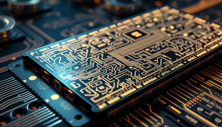
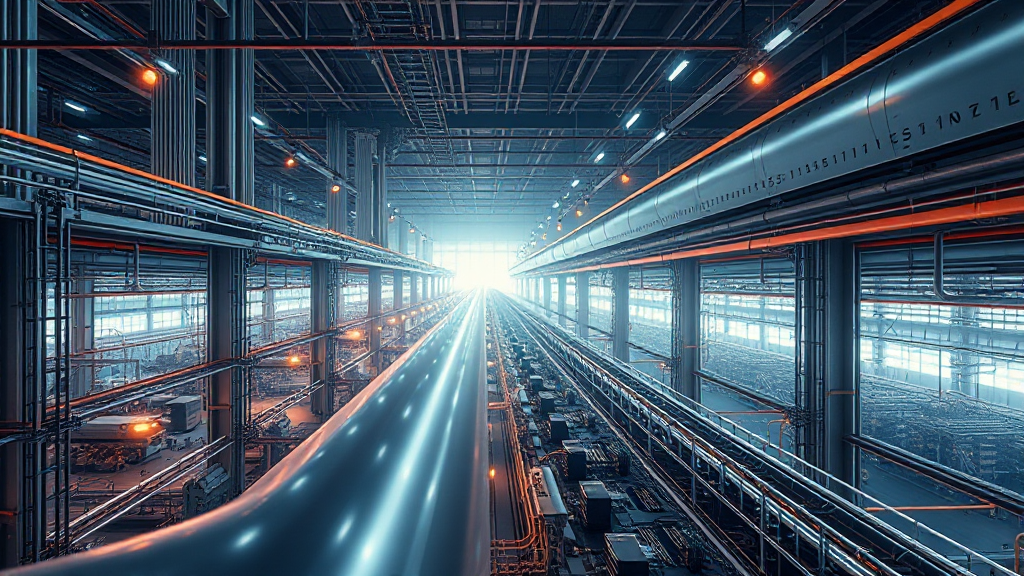
Architecture & Packaging: Under One Roof at Terafab
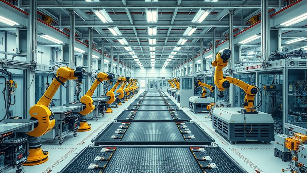
The standard semiconductor pipeline relies on a highly fragmented flow. Wafers are printed in Taiwan, memory stacks are built in Korea, and packaging occurs at outsourced semiconductor assembly and test (OSAT) sites across Southeast Asia. The Terafab project, officially announced by Elon Musk on March 21, 2026, attempts to collapse this geography into a single, vertically integrated manufacturing loop.
[Silicon Wafer Prep] ──> [Intel 14A Logic Fab] ──┐
                                                 ├─> [In-House Advanced Packaging (2.5D/3D)] ──> [Tested Compute Modules]
[Memory Substrate] ───> [Co-Packaged HBM Stack] ─┘
The physical layout of the prototype facility on the North Campus of Giga Texas consolidates lithography, logic fabrication, high-bandwidth memory (HBM) stacking, and 2.5D/3D assembly under one roof. This design is engineered to slash the cycle time for custom silicon revisions from the typical 90-day industry standard down to single-digit days.
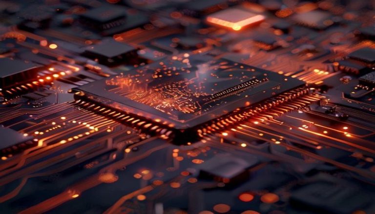
For Tesla chip manufacturing, the physical architecture of the target silicon demands advanced packaging solutions that Tesla has never managed in-house. To achieve the 1 Terawatt (1 trillion watts) per year of AI compute targeted by the venture, the primary silicon engine must combine dense logic chiplets with custom HBM stacks. The integration utilizes an embedded multi-die interconnect bridge (EMIB) design licensed from Intel, which allows sub-10-micron interconnect pitches between the logic and memory dies.
Unlike standard 2.5D packaging that relies on a passive silicon interposer, this EMIB-based architecture uses small silicon bridges embedded directly within an organic substrate. This layout reduces total die area and avoids the reticle-limit constraints of large silicon interposers.
However, the thermal mechanics of this integrated package present severe challenges. Combining logic dies pulling over 700 watts with thermal-sensitive HBM stacks requires precise microfluidic cooling channels or advanced silicon micro-vias to prevent thermal throttling.
Furthermore, the physical footprint of the memory interface is highly constrained. By placing the memory controller directly adjacent to the compute tiles, the design minimizes latency but increases substrate routing density to levels where cross-talk and electromagnetic interference threaten signal integrity. Gary Jiang’s background in managing the mechanical stress, warpage, and alignment tolerances of the 18A node is designed to mitigate these exact structural defects.
Perf/W & Benchmarks: Intel 14A Versus the Competitors
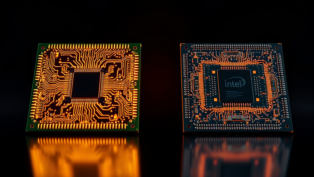
The performance targets for Tesla chip manufacturing rely heavily on the physical properties of Intel’s 14A process node. Intel designed 14A to deliver a 15% to 20% performance-per-watt improvement at constant power, or a 25% to 35% power reduction at equivalent performance when compared to the 18A node.
| Metric | Intel 18A | Intel 14A | TSMC A14 |
|---|---|---|---|
| Transistor Type | RibbonFET (GAA) | RibbonFET 2 | Nanosheet GAA |
| Power Delivery | PowerVia (Backside) | PowerDirect | Super Power Rail (A12) |
| Lithography | Low-NA EUV (0.33 NA) | High-NA EUV (0.55 NA) | Low-NA EUV Multipatterning |
| Logic Density Delta | Baseline | +30% | +15-18% |
| Expected HVM Year | Late 2025 / 2026 | 2028-2029 | 2028 |
Intel’s 14A architecture introduces two primary physical innovations: RibbonFET 2 and PowerDirect. RibbonFET 2 is Intel’s second-generation gate-all-around (GAA) transistor structure, which improves electrostatic control over the channel and lowers the minimum operating voltage (V_{min}). PowerDirect is a refined backside power delivery network. By moving the power delivery circuitry to the backside of the wafer, Intel decouples the power grid from the signal routing on the front side. This design lowers resistive losses (I^2R drop), improving power efficiency by up to 15% while freeing up critical routing resources for the signal layers.
Furthermore, Intel’s implementation of “Turbo Cells” within the 14A node accelerates critical timing paths in high-frequency compute clusters without increasing the overall footprint of the die. These double-height, high-drive cells are strategically integrated into the design layout, allowing the chip’s arithmetic logic units (ALUs) to scale frequency under heavy workload cycles.
When applied to transformer-based workload execution, such as those used in Tesla’s Full Self-Driving (FSD) stack and xAI’s language models, these physical properties alter the cost-per-flop metric. High-drive cells combined with backside power delivery allow the chip to maintain peak performance without entering the thermal-runaway states common in traditional FinFET structures.
Is the physical choice of Intel 14A superior to TSMC’s A14 roadmap? TSMC chose a more conservative path, electing to skip High-NA EUV for its A14 node to prioritize cost efficiency and avoid the tool-integration risks of ASML’s newest hardware. TSMC relies on complex low-NA EUV multi-patterning. This method maintains high yields but introduces lithographic variability and edge placement errors across multiple exposures.
Intel’s High-NA EUV single-exposure approach on 14A, by contrast, resolves features down to 8nm in a single pass. This single-exposure patterning significantly reduces cycle times and defect density, but it forces a massive upfront capital premium. For Tesla, this technical choice means the silicon could theoretically outperform TSMC-manufactured competitors in raw compute density, provided the physical yield curve stabilizes.
These physical performance deltas are comparable to the silicon efficiency gains observed in the broader industry. For instance, customized accelerators have shown how optimizing the underlying silicon can drastically alter cost dynamics [OpenAI Custom Chip Slashes LLM Costs by 50%]. Tesla expects a similar efficiency step-function, projecting that custom 14A architecture will deliver a major reduction in per-token inference costs for its Dojo and FSD networks.
Yield, Cost, and Capacity: The $119B Financial Engine
The economic scale of the Terafab project is unprecedented for a private technology conglomerate. While Elon Musk initially framed the venture as a $20 billion prototype, filings and public hearings in Grimes County, Texas, revealed a far larger multi-stage commitment. SpaceX’s S-1 filings peg the initial capital expenditure for the prototype phase at $55 billion, with total investments across all expansion phases projected to reach $119 billion.
                                      [Capex Target]
Phase 1: Austin Prototype  ──>  $55 Billion Capital Investment  ──> 100,000 Wafers/Month
Phase 2: Grimes County     ──>  $64 Billion Capital Investment  ──> 1,000,000 Wafers/Month
                                ──────────────────────────────
                                Total: $119 Billion
The baseline economic driver of this investment is wafer throughput. The Austin prototype facility is designed to target 100,000 wafer starts per month (WSPM) using the Intel 14A process. The planned Grimes County site is engineered to scale to a staggering 1 million WSPM. For perspective, a 100,000 WSPM fab matches the output of TSMC’s largest gigafabs.
Operating at this level requires an continuous supply of ASML Twinscan EXE:5200B High-NA EUV systems. With each system priced at approximately $380 million, outfitting a fab to run 100,000 WSPM requires a minimum of 10 to 15 scanners, translating to 3.8 billion to 5.7 billion in lithography equipment alone.
The fundamental risk to the financial engine of Tesla chip manufacturing is the early-stage yield curve. Advanced node wafer prices for Intel 14A are estimated to exceed $25,000 per wafer, driven by the massive depreciation costs of High-NA EUV tooling. If early yields hover around 30% to 40% during risk production, the effective cost per working die increases dramatically.
Cost Per Working Die = Total Wafer Cost / (Total Dies per Wafer * Yield Rate)
At 30% Yield: Effective Die Cost is ~3x the Baseline Cost.
To achieve profitability, Gary Jiang must accelerate the yield ramp. During his tenure at Intel, 18A yields reportedly rose at a rate of roughly 7% per month. Replicating this rate on the more complex 14A process at Tesla will require optimizing the lithographic overlay precision down to the target 0.7nm threshold.
[Yield Optimization Loop]
   │
   ├──> [0.7nm Overlay Precision Alignment]
   ├──> [Directed Self-Assembly Defect Reduction]
   └──> [Real-Time Metrology Feedback]
How does Tesla plan to amortize these staggering investments? The compute generated by the completed wafers is intended for internal consumption across Tesla, SpaceX, and xAI. The targeted 1 Terawatt of compute per year is equivalent to several hundred state-of-the-art supercomputers running simultaneously.
This sheer volume of processing power mirrors the infrastructure scale seen in the world’s most advanced computing installations [Enterprise AI deployment at HP yields 3 massive results]. Rather than purchasing hundreds of thousands of Nvidia GPUs at a massive retail premium, Tesla plans to manufacture its own silicon at a lower unit cost, aiming to offset the $119 billion capital layout over a ten-year operational window.
Supply Chain Dynamics: Navigating the High-NA EUV Bottleneck
To establish a functional domestic fab, Tesla must secure access to a highly concentrated supply chain. ASML remains the sole global source for the High-NA EUV scanners required for the 14A process, producing only five to six units annually.
Intel secured the earliest shipment slots, giving it a temporary lead in High-NA tool installation. By partnering with Intel on the Terafab project, Tesla gains indirect priority access to these hard-to-source tools. This partnership protects Tesla from the multi-year equipment lead times that would occur if it attempted to negotiate directly with ASML as an independent foundry.
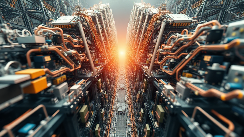
The logistics of setting up these massive machines are incredibly demanding. A single Twinscan EXE scanner is roughly the size of a double-decker bus, weighs over 150 metric tons, and requires three Boeing 747 cargo planes to transport in pieces.
Once on-site in Austin, the tool must be calibrated in an ultra-clean environment with absolute vibrational isolation. The local power infrastructure must also support the scanner’s massive energy footprint; the laser system alone uses several megawatts of power to vaporize tin droplets into the plasma that generates the 13.5nm EUV light.
Beyond lithography, the supply chain for advanced packaging materials is concentrated in a handful of key firms. Substrates like Ajinomoto Build-up Film (ABF) are subject to chronic industry-wide shortages, with lead times frequently extending past 12 months. Any disruption in the supply of high-purity chemicals, specialized photoresists, or silicon carrier wafers will immediately stall the Terafab assembly line.
By centering its manufacturing footprint in Texas, Tesla attempts to insulate its operations from the geopolitical risks of the Taiwan Strait. This strategic onshore move is similar to other hardware developers trying to secure proprietary supply lines [Nvidia AI Competitors Strike With 2 Bold Tech Acquisitions]. If Tesla can successfully secure its supply of substrates and high-purity raw materials within North America, it will establish an exceptionally resilient hardware ecosystem.
Forward Vector: The Next 18 Months

As the Terafab project transitions from structural design to active tool installation under Gary Jiang, several critical technical checkpoints will determine the project’s viability.
                                 [PROJECT TIMELINE]
     Q3 2026                 Q4 2026                 H1 2027                 H2 2027
        │                       │                       │                       │
        ▼                       ▼                       ▼                       ▼
[Gary Jiang On-site] ──> [Intel 14A PDK 0.9] ──> [First Test Shuttle] ──> [Tool Calibration]
     (Austin, TX)           (October 2026)         (Silicon Run)          (Austin Prototype)
- Checkpoint 1: The October 2026 PDK 0.9 Release: This is the most immediate gating item. Intel is scheduled to deliver the 14A Process Design Kit (PDK) version 0.9 to external customers in October 2026. Tesla’s design teams must use this kit to map their custom silicon layouts to the physical design rules of the 14A process. Any delay in this software release will push out the tape-out schedule for the first test silicon.
- Checkpoint 2: First Test-Shuttle Silicon Runs (H1 2027): Once the design rules are locked, Tesla must run its first experimental test chips through Intel’s development fabs. These runs will verify whether the GAA RibbonFET 2 transistors and PowerDirect backside power delivery perform according to simulated benchmarks.
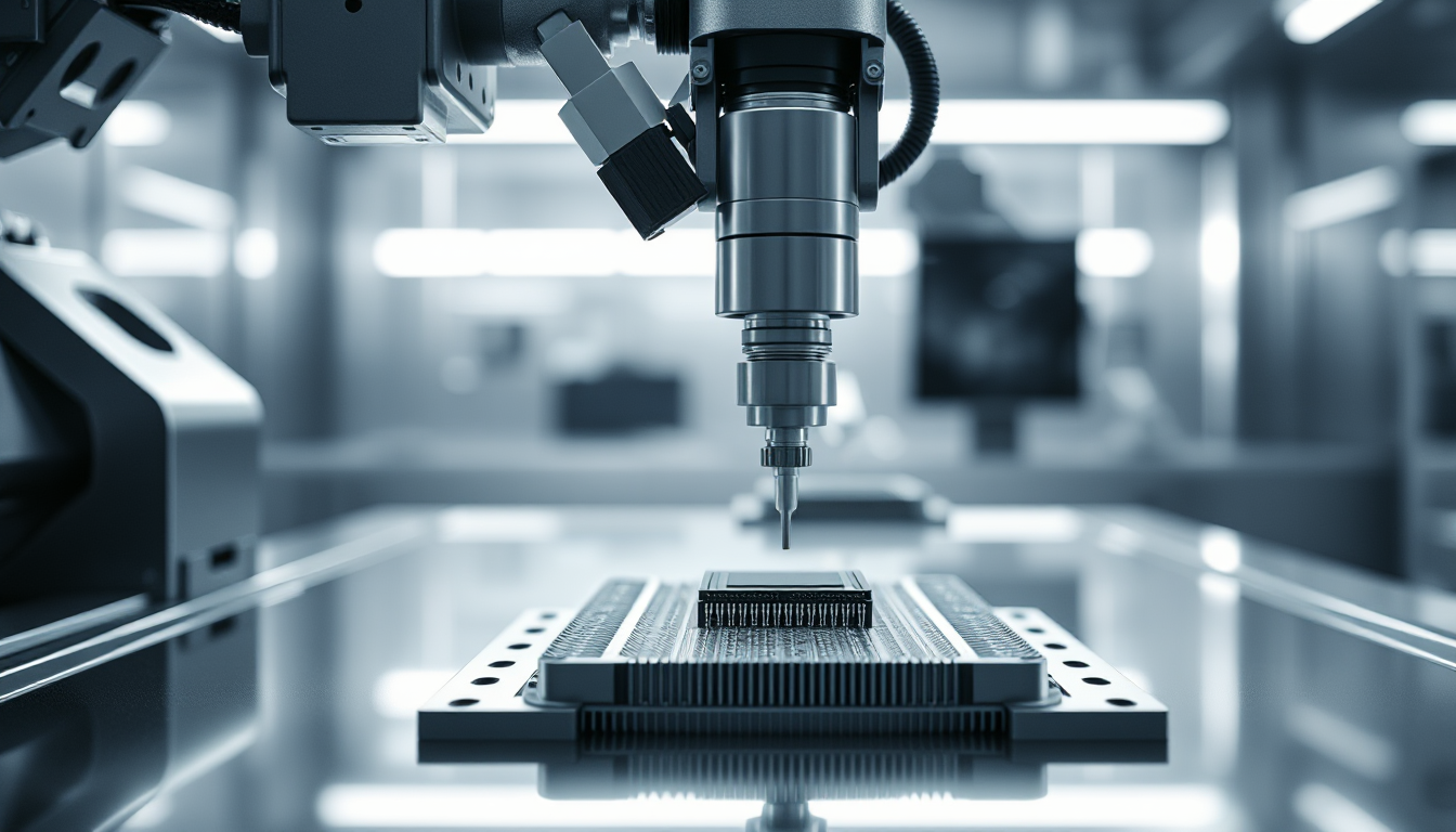
- Checkpoint 3: Tool Calibration and Cleanroom Certification in Austin (H2 2027): As physical construction of the Austin prototype facility nears completion, Jiang’s team must install and calibrate the lithography and packaging tools. This includes certifying the cleanroom to Class 1 standards (less than 10 particles per cubic meter of air) and stabilizing the High-NA EUV optical columns against local seismic activity.
- Checkpoint 4: Directed Self-Assembly (DSA) Validation (Ongoing): Intel’s 14A node is planned to combine High-NA EUV with Directed Self-Assembly, using chemical block copolymers to form ultra-fine lines. Managing the defect density of this hybrid lithography process will be a continuous challenge for the engineering team.
If these checkpoints are met, the first functional custom silicon from Tesla chip manufacturing could begin risk production by early 2028, paving the way for full-scale vertical integration. However, any failure in tool calibration or severe yield drops below 50% will quickly inflate the capital burn rate, testing the financial limits of even Musk’s vast corporate empire.
Frequently Asked Questions
What is the scale of the new tesla chip manufacturing facility?
The Terafab project begins with a $55 billion prototype facility on the North Campus of Giga Texas in Austin, designed for 100,000 wafer starts per month. The planned full-scale complex in Grimes County, Texas, is designed to cover 10 million square meters (110 million square feet) with an ultimate target capacity of 1 million wafer starts per month.
Why did Tesla hire Gary Jiang from Intel?
Tesla hired Gary Jiang because of his extensive hands-on experience in managing leading-edge semiconductor fabs. He spent nearly 18 years at Intel, most recently serving as a Factory Manager responsible for the tool installation, facility construction, and technology transfer of Intel’s advanced 18A process node.
What process node is the Terafab targeting?
The Terafab project is partnering with Intel to utilize the Intel 14A (1.4-nanometer class) process node. This node features next-generation RibbonFET 2 gate-all-around transistors, PowerDirect backside power delivery, and relies on ASML’s Twinscan EXE:5200B High-NA EUV lithography.
References
- Electrek: Tesla poaches 17-year Intel veteran to lead its ‘Terafab’ chip plant (June 30, 2026).
- TradingView: Tesla Ropes In Intel Veteran To Lead Elon Musk’s Ambitious Terafab Project (July 1, 2026).
- AnySilicon: Intel Begins Work on 10A and 7A Process Nodes as 14A Roadmap Moves (May 2026).
- TechPowerUp: Intel 14A Node Expected to Cost More Than 18A, Driven by High-NA EUV (September 2025).
- Digitimes: Intel completes high-NA EUV validation for 14A, advances 2D transistor tech (December 2025).
- AI Weekly: Intel Promises Apple and Terafab a 14A PDK Milestone This Fall (June 2026).
- TrendForce: Intel Tapped as Tesla Wins First 14A Customer Spot in Terafab Push (April 2026).
- AI Magazine: Why has Elon Musk Partnered with Intel on Terafab? (April 2026).